C.9.3 Dielectric material discharge.
C.9.3.1. General
Dielectric material discharge deals with the case when, during a breakdown, the electrons come from a charged dielectric.
Punch through is the classic breakdown of a dielectric material, a phenomenon which can occur in the breakdown of a capacitance, for example. For surface charging, the material is pierced right through its depth, the charges accumulated on either side of the surface recombining by this path.
Flash-over is a surface discharge which is propagated from a starting point. The surface of the dielectric becomes conductive (by creation of a plasma), and the discharge current closes in on the closest electric ground (metallization of the dielectric in most of the cases). The surface discharge current returns to ground by the edge of the material.
Blow-off concerns the emission of negative charges (electrons) into space. These emitted electrons can reach a satellite electric ground, far away from the emission site. The phenomenon occurs simultaneously with the flash-over and is proportionally linked to it.
C.9.3.5. Discharge theory
At first, the dielectric undergoing the bombardment of the electrons coming from the plasma "traps" some of them inside the material very close to the surface. These electrons accumulate in trap sites, forming a negative layer in the material. The accumulation of these electrons over a length of time generates intense electric fields inside the dielectric which can lead to the appearance of the punch through phenomenon. The flash-over and blow-off phenomena then begin to occur as illustrated schematically in Figure C-6.
The propagation of the discharge requires a transverse field (parallel to the surface of the material) and a desorbed gas.
This gas can be supplied during the punch through. Indeed, at punch through, the energy released inside the material raises the temperature of this material, causing a conductive plasma to appear.
Under the effect of the transverse field, a neutral atom is separated into an ion and an electron. The electron rejoins the surrounding ground and the ion compensates the electronic charge by settling on the surface of the dielectric thus desorbing an atom. This atom is in turn ionized and the process can be repeated until total compensation of the charges.
The discharge is thus propagated over the entire surface of the dielectric like a bush fire.
The discharge therefore leaves behind a double layer which takes tens of minutes to neutralize.

Figure C-6: Dielectric discharge mechanism.
While flash-over takes place, the blow-off phenomenon appears. In contrast to flash-over, which is a purely local phenomenon, and which consequently cannot create a current outside the dielectric, the electrons issued from blow-off follow settle on the surrounding structures where they then circulate. Blow-off electrons generate discernible and measurable currents. The positive image charges found in the metallization of the dielectric support is neutralized by a current of electrons which travels from the satellite structure towards the metallization of the dielectric: it is an electrostatic re-equilibrating current
As shown in Figure C-7, the discharge starts at a point in the sample generally having a defect, and then moves away radially from this point. The circular discharge edge mobilizes an increasingly large part of the sample until it reaches the edges. At that moment, the discharge current decreases.

Figure C-7:Shape of the current in relation to discharge starting point.
The discharges that generally last several hundred nanoseconds, have amplitudes of around 1000 amps per linear metre of discharge and raising edges of 106 to 108 A/s, this data varying, as we have just seen, according to the materials, to their size, to their shape and to the starting point of the discharge. An example of a discharge wave-form is shown in Figure C-8.

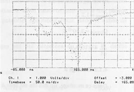
Figure C-8 : Example of discharge on pierced aluminized Teflon® irradiated by electrons with energies ranging from 0 to 220 keV.